
For as often as TSMC has extolled the virtues of FinFET chip designs, we've been wondering exactly when we'd find them sitting in our devices. Thanks to competition from rival semiconductor firms, we'll get them relatively soon: the company now expects to produce its first wave of FinFET-based, 16-nanometer chips toward the end of 2013. While they won't be as nice as 14nm-XM chips in the pipeline, the 16nm parts should still offer battery life and speed improvements over the 28nm chips we know today. These improvements also won't be the end of the road -- TSMC anticipates 10nm designs built on extreme ultraviolet lithography late into 2015, and CEO Morris Chang believes there's seven or more years of advancements in manufacturing before Moore's Law starts breaking down. We'll just be happy if we see FinFET reach our phones and tablets in the near term.
Filed under: Cellphones, Tablets
Comments
Via: Phone Arena
Source: EETimes
 Samsung has finally nailed a much-anticipated chip manufacturing technique that will help phones perform faster and keep their batteries juiced for longer. The company is now building 7-nanometer chips using extreme ultraviolet (EUV) technology -- a...
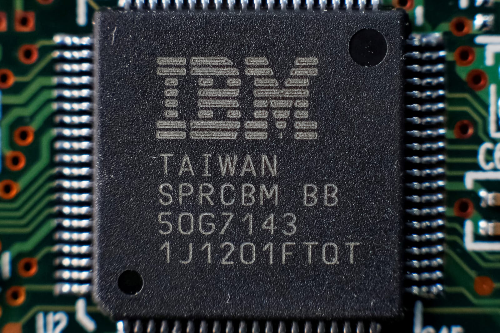 Who said Moore's Law was dead? Certainly not IBM or its chip partners Globalfoundries and Samsung. The trio has developed a transistor manufacturing process that should pave the way for 5-nanometer chips. While the team etched the chip using the same...
