
CCD sensors have long ruled the digital imaging roost, but a team of researchers at Johannes Kepler University in Linz, Austria have concocted flat, flexible and transparent image sensors that could eventually change things up. Made from a flexible polymer film suffused with fluorescent particles, the prototypes catch only a specific wavelength of light and shoot it to an array of sensors that surround the sheet's edge. At that point, the rig calculates where light entered the polymer by measuring how much it has diminished during its travel time, and then composes an image from that data. It's said the process is similar to how a CT scan functions, but uses visible light instead of X-rays. Not only is the membrane relatively inexpensive and potentially disposable, but the solution is a world's first, to boot. "To our knowledge, we are the first to present an image sensor that is fully transparent - no integrated microstructures, such as circuits - and is flexible and scalable at the same time," said Oliver Bimber, co-author of the group's paper.
As of now, the setup only snaps black and white images with a resolution of 32 x 32 pixels, but there are plans to boost its fidelity by leveraging higher quality photodiodes (or even composite photos). Also, color photographs could be achieved by using several sheets that capture different hues of light. So, what's this all mean for practical applications? Researchers believe its prime use lies in layering the film on TV screens and other displays to offer gesture controls without pesky, additional cameras. In addition, objects can be imbued with sensor capabilities if wrapped with the layer, and even CCD's could benefit from having a slice of the polymer slapped on them to take photos at different exposures. Hit the second source link for the scientific nitty-gritty, or head past the break for a glimpse at the setup's photos.
Filed under: Cameras, Alt
Comments
Via: Gizmodo
Source: The Optical Society, Optics InfoBase
 Samsung's latest smartphone camera sensor above is under 5mm wide, but it has a resolution of 43.7 megapixels -- more than most DSLRs. That means the pixels on the "Isocell Slim GH1" are just 0.7 micrometers wide, beating the 0.8-micrometer pixels on...
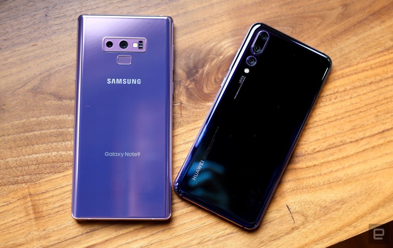 With its chip manufacturing prowess, it was only a matter of time before Samsung attacked the lucrative image sensor market dominated by Sony. It has unveiled a pair of very interesting sensors aimed at multi-camera smartphones, the 48-megapixel Isoc...
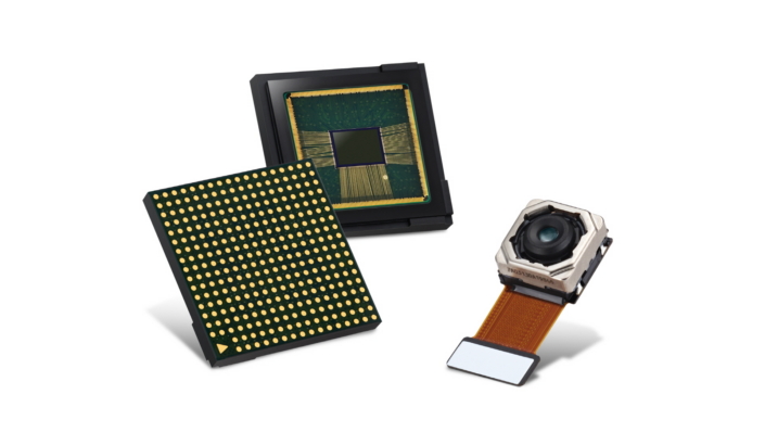 Today, Samsung announced that the 16-megapixel ISCOCELL Slim 3P9 image sensor is now available. This image sensor is designed for cameras on mobile devices; because of its Tetracell technology, this 1.0μm sensor can work as a 2.0μm in front-fac...
 It's been over five years since we heard from InVisage, a company developing a new kind of smartphone sensor with higher dynamic range and zero rolling shutter. It just produced a short film called Prix using a prototype chip to show exactly how th...
 Toshiba's accounting scandal may cost it a lot more than just a CEO and a wad of cash. Sources for Bloomberg, the Japan Times and Reuters all claim that the tech giant is expected to sell its camera sensor business (specifically, its manufacturing...
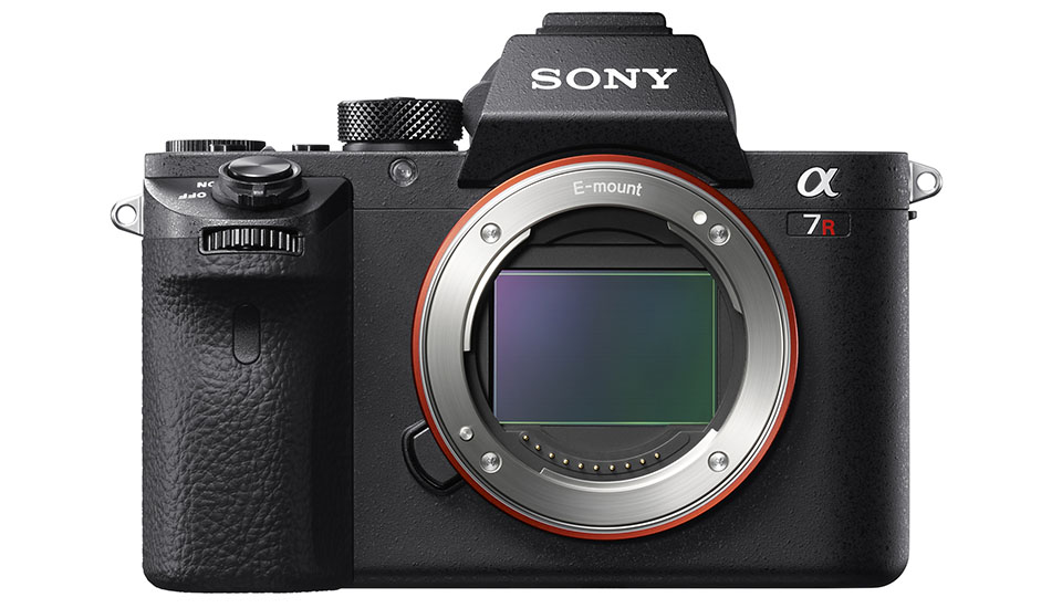 Sony is transforming one of its most successful businesses, image sensors, into a brand new company called Sony Semiconductor Solutions. All of its chips will be produced under the new company, but Sony said in a statement that "image sensors are a...

