
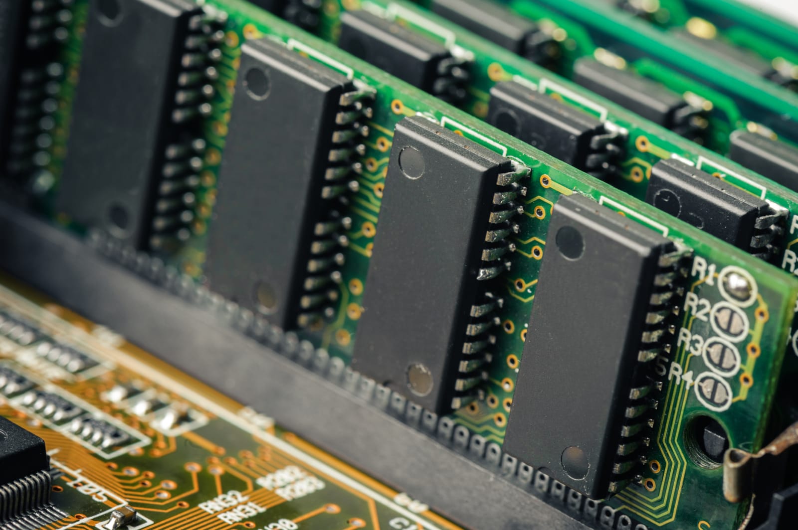
Pretty much the only place you see vacuum tubes any more is inside a quality audio amp. But, once upon a time, they were the primary ingredient in any piece of electronic equipment, including computers. The glass tubes have since been replaced with the smaller, less fragile and cheaper to manufacture silicon transistor. There are, however, disadvantages, to transistors. For one, electrons tend to move more slowly though the semiconductors, and two, they're highly susceptible to radiation. The second of those problems doesn't affect us much here on Earth, but for NASA it poses a major obstacle. Engineers have finally managed to combine the advantages of both vacuum tubes and silicon transistors, though, in what has been dubbed "nano vacuum tubes." They're created by etching tiny cavities in phosphorous-doped silicon, bordered on three sides by electrodes that form the gate, source and drain. The term "vacuum tube" is slightly misleading however, since there is no true vacuum in play. Instead, the source and drain are separated by just 150 nanometers, making it highly unlikely that flowing electrons would run into stray atoms. In addition to their space-worthy hardiness, they can also potentially operate at frequencies ten-times as higher than silicon transistors, making them a candidate to push terahertz tech from experimental to mainstream. For more, check out the source link.
[Image credit: Shane Gorski]
Nano vacuum tubes could give a second life to the guitarist's best friend originally appeared on Engadget on Sun, 27 May 2012 17:36:00 EDT. Please see our terms for use of feeds.
Permalink  DVICE
DVICE |
 ScienceNOW
 |
Email this |
Comments
 Never mind the possibilities opened up by millimeter wave 5G and other many-gigahertz technologies -- the FCC is already thinking about the next generation beyond that. The Commission has voted unanimously in favor of creating a category of experime...
 Chicken hatcheries often grind up male chicks as soon as they break out of their shells -- they don't produce enough meat as adults, so they're considered useless compared to the egg-laying females. It's not exactly compassionate, and it wastes mone...
 One area limiting speed in personal computing speed is memory -- specifically, how quickly individual memory cells can be switched, which is currently done using an external magnetic field. European and Russian scientists have proposed a new method u...
 There are some books that are simply too delicate to crack open -- the last thing you want to do is destroy an ornate medieval Bible simply because you're curious about its contents. If MIT has its way, though, you won't have to stay away. Its scient...
 Terahertz radiation, or T-rays, can do some really incredible stuff. It can be used to scan for tumors and bombs build ultrafast wireless networks and see through solid objects. As an imaging technology, however, T-ray cameras have always had a resol...
 Terahertz spectrum scanning is potentially ideal for finding bombs due to the sheer range of materials it can detect, but it's not exactly practical for luggage checks when you need both a suitcase-sized machine and up to half an hour to conduct a sc...


